RENA Technologies commissions high-tech-processing facility for TGV glass substrates
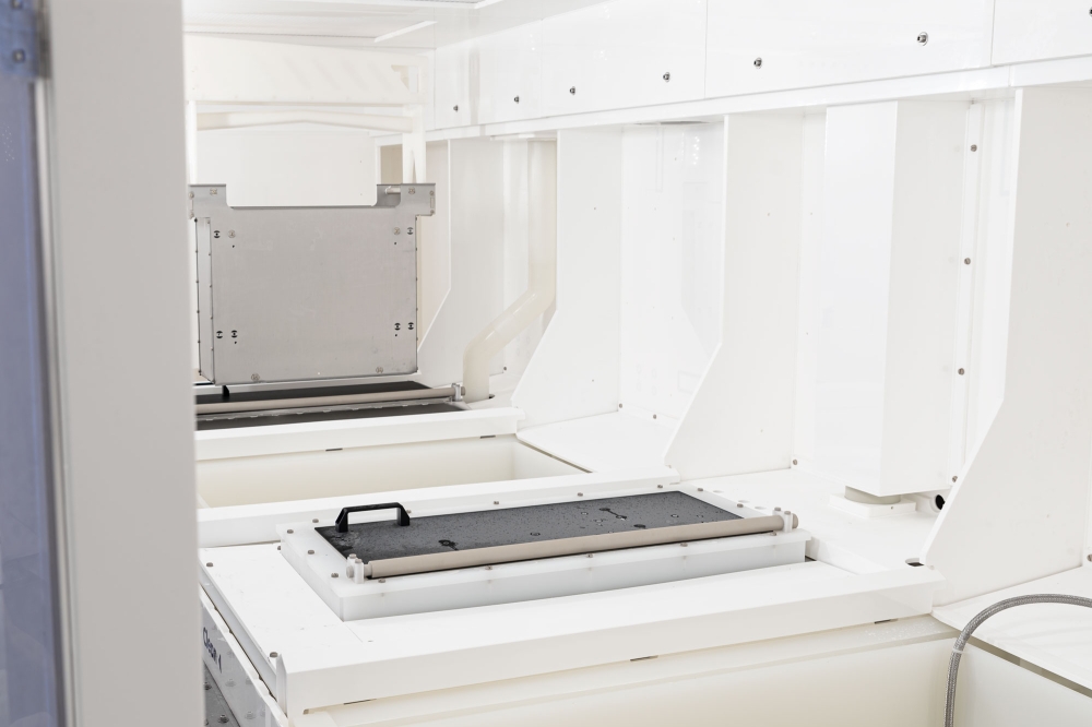
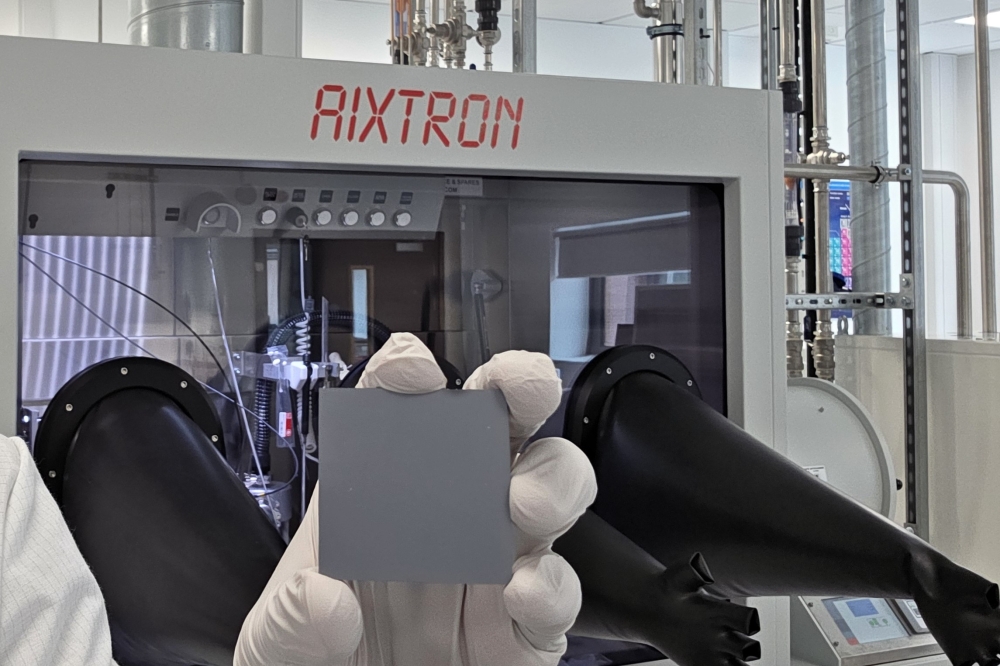
RENA Technologies, a leading manufacturer of wet processing equipment for semiconductor and advanced packaging production, has announced the ramp-up of its dedicated glass core substrates facility in Germany. This new line, designed for substrates up to 510 × 515 mm, immediately opens for customer test lots, underscoring RENA's proven expertise in glass processing and creating new opportunities for process development and customer sample production.
“As experts in precision wet processing, we can now offer large panel demo services for high aspect ratio through glass via (TGV) formation on various glass types,” said Dr. Holger H. Kuehnlein, SVP Technology at RENA. “Our alkaline based TGV process delivers extremely small taper angles, low sidewall roughness, and exceptional dimensional control at panel scale, enabling high density via applications. Customers can begin validating these capabilities today.”
Why Glass, and Why Wet Processing?
Glass substrates offer significant advantages for advanced electronics, including ultra-flat surfaces, low dielectric loss, and superior thermal stability. However, realizing these benefits at scale requires defect free surface preparation and the formation of uniform, high density TGVs with minimal taper angles. RENA`s wet processing systems are specifically designed to address both challenges:
1. Surface Engineering – Our systems ensure precise cleaning and stress relief across 600 x 600mm panels with submicron total thickness variation (TTV).
2. Chemically Formed TGVs – Following initial laser modifications performed by specialist partners, RENA’s proprietary chemistries form, enlarge and shape each via to
exact specifications. This process consistently delivers very small taper angles and smooth sidewalls, ideal for subsequent metallization.
By collaborating with leading German and international laser partners, RENA offers customers the flexibility to choose their preferred laser vendor while ensuring all downstream wet processing steps are handled by our advanced equipment.
Market Impact
High-Performance Computing (HPC) as well as 5G/6G RF modules increasingly require new package designs, including panel-level fan-out and trend towards more complex chiplet architectures. Glass substrates, long considered the “holy grail” for core and interposer material, effectively eliminate the limitations imposed by warpage and dielectric loss in organic substrates. By combining laser modification from our vetted partners with RENA’s chemistry driven via shaping, designers can now validate glass packaging concepts on the lab-platform proven at 600x600mm dimensions.
“With this lab-tool, we've created a great opportunity for semiconductor manufacturers to perform demos on panel level glass substrates,” added Peter Schneidewind, CEO of RENA. “From surface preparation to via formation, our wet process flow is ready for customers substrates to support TGV technology breakthroughs. This is world class made in Black Forest”